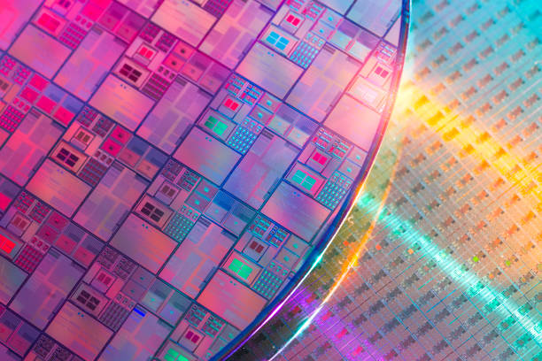
Patterned wafers serve as the backbone of modern electronics, enabling the creation of increasingly powerful and compact devices. These wafers are typically made from semiconductor materials, such as silicon, which possess unique electrical properties.
Through a series of intricate manufacturing processes, patterned wafers transform from raw materials into functional devices, paving the way for technological advancements.
The Importance of Design in the Manufacturing Process

Source: istockphoto.com
Design is a critical factor in the successful manufacturing of patterned wafers. Skilled engineers and designers meticulously create and optimize the layout of circuits and devices on Patterned Silicon Wafers, considering factors such as performance, power consumption, and manufacturability.
By employing computer-aided design (CAD) software and simulation tools, designers can simulate and analyze the behavior of circuits before they are physically fabricated. This iterative design process helps refine and optimize the layout, ensuring that the final product meets the desired specifications.
Semiconductor Materials and their Role in Patterned Wafers
Semiconductor materials are at the heart of patterned wafers, providing the foundation for electronic devices. Silicon is the most widely used semiconductor material due to its abundance and excellent electrical properties.
However, depending on the specific application, other materials like gallium arsenide (GaAs), indium phosphide (InP), or gallium nitride (GaN) may be employed. These materials offer distinct advantages in terms of performance, efficiency, or operating temperature range.
The choice of a semiconductor material depends on factors such as the intended device functionality, target market, and manufacturing constraints. Each material has its unique characteristics, including carrier mobility, bandgap energy, and thermal conductivity, which influence the performance and behavior of the resulting devices.
Photolithography: Creating Patterns
Photolithography is a key process in patterned wafer manufacturing, enabling the creation of precise patterns on a large scale. The process begins with a clean surface, ensuring the absence of contaminants that could affect the pattern replication. A thin layer of photoresist is then applied uniformly over the wafer.
To define the patterns, the disk is exposed to UV light through a mask. The mask contains the desired pattern, and the UV light selectively exposes the photoresist in specific areas. The exposed photoresist undergoes a chemical transformation that makes it either more soluble or less soluble in a developer solution.
After exposure, the wafer is immersed in a developer solution, which selectively removes either the exposed or unexposed areas of the photoresist, depending on the type of resist used. This step reveals the desired patterns on the surface. The remaining photoresist acts as a protective layer during subsequent processes, such as etching or deposition, ensuring that the patterns are faithfully transferred to the underlying materials.
Etching and Deposition Processes for Pattern Transfer
Once the patterns are defined through photolithography, etching and deposition processes come into play to transfer the patterns onto the wafer’s surface. Etching is a process of selectively removing materials, either through chemical reactions or physical means.
Different types of etching techniques, including wet etching, dry etching, and plasma etching, are employed based on the materials being etched and the desired precision.
Deposition processes, on the other hand, involve adding new materials to the wafer’s surface. Physical vapor deposition (PVD) utilizes techniques like sputtering or evaporation to deposit thin films of materials onto the disk. Chemical vapor deposition (CVD) involves the reaction of gases to form a solid film on the surface. These deposition techniques are crucial for creating the desired structures, such as metal interconnects, dielectric layers, or semiconductor junctions.
Metrology and Quality Control in Manufacturing
Metrology and quality control play a vital role in ensuring the accuracy and reliability of patterned wafers. Metrology involves the precise measurement and characterization of various parameters, including critical dimensions, material properties, and surface topography.
Advanced metrology tools, such as scanning electron microscopes (SEM), atomic force microscopes (AFM), and optical profilers, enable manufacturers to perform detailed inspections and measurements.
By carefully analyzing the measurements obtained through metrology, manufacturers can assess the conformity of the patterned wafers to the design specifications. Deviations from the intended dimensions or patterns can be identified and addressed promptly, ensuring that the final product meets the required quality standards. These quality control measures help reduce defects, enhance yield, and improve overall process efficiency.
Emerging Technologies in Patterned Wafer Manufacturing

Source: everythingrf.com
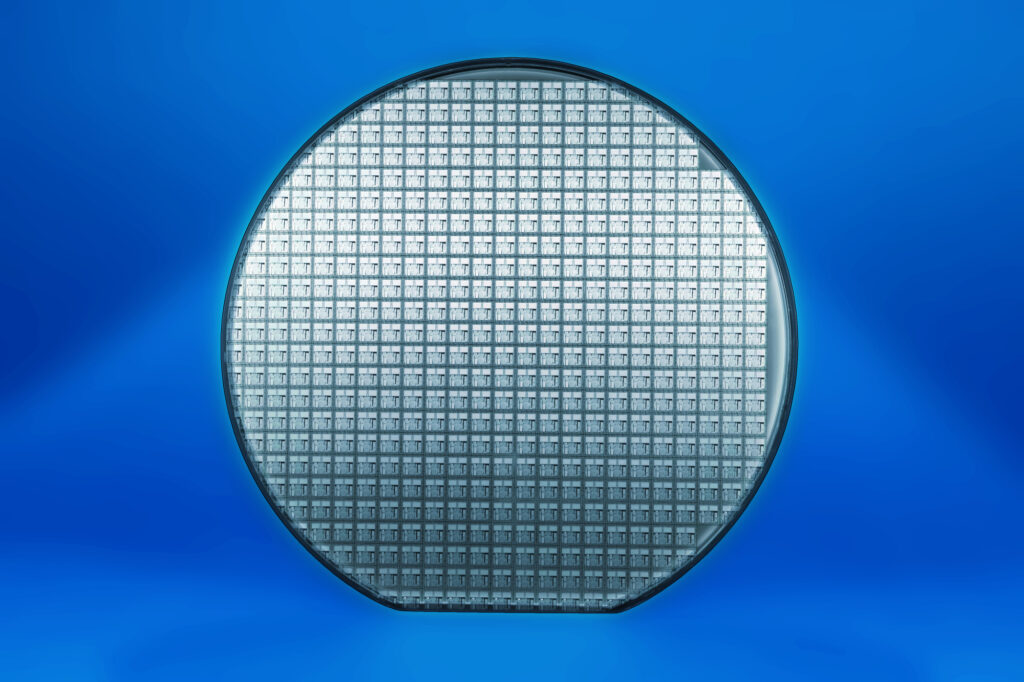
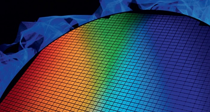
As technology continues to advance, new manufacturing techniques and technologies are emerging in patterned disk production. One such innovation is extreme ultraviolet lithography (EUVL), which utilizes ultrashort-wavelength EUV light to create smaller features with higher precision. EUVL allows for more precise patterning, enabling the production of advanced semiconductor devices with improved performance.
Directed self-assembly (DSA) is another promising technology in patterned wafer manufacturing. DSA involves the use of self-assembling block copolymers, which can spontaneously arrange themselves into nanoscale patterns. This technique offers a cost-effective and scalable approach for creating sub-10-nanometer features, complementing traditional lithography processes.
Nanoimprint lithography (NIL) is also gaining attention as an alternative patterning technique. It involves using a mold to press patterns into a resist-coated wafer, creating precise patterns through mechanical deformation. NIL offers high resolution and the potential for cost-effective replication of patterns over large areas.
These emerging technologies hold the potential to overcome existing challenges in patterned wafer manufacturing and open up new possibilities for advanced semiconductor devices with enhanced performance and functionality.
Case Studies: Real-World Applications of Patterned Wafers

Source: ebay.ca
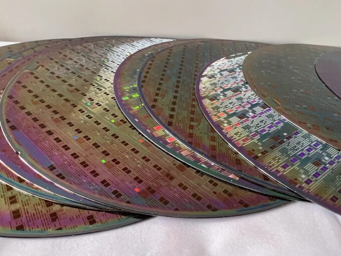
Patterned wafers find applications in various industries, playing a crucial role in advancing technology and enabling a wide range of electronic devices. In the consumer electronics industry, patterned wafers are utilized in the production of smartphones, tablets, and wearable devices. The intricate circuits and miniaturized components on these disks make it possible to incorporate advanced functionalities and high-performance features into compact form factors.
The telecommunications industry heavily relies on patterned wafers for the production of communication devices, including routers, modems, and optical networking equipment. These devices require precise patterns and high-speed circuitry to ensure efficient data transmission and network connectivity.
The automotive sector also utilizes patterned wafers for various applications, such as advanced driver-assistance systems (ADAS), infotainment systems, and electric vehicle components. Patterned plates enable the integration of sensors, microcontrollers, and power electronics, contributing to enhanced safety, performance, and energy efficiency in vehicles.
In the healthcare industry, patterned wafers play a crucial role in medical imaging devices, biosensors, and implantable medical devices. These disks enable the miniaturization of devices, enhancing portability and patient comfort while maintaining high accuracy and performance.
Conclusion
Patterned plates are a complex but powerful tool for the semiconductor industry. From design to reality, there is a lot that goes into understanding and executing the manufacturing process of these patterned wafers.
By mastering all of its elements in detail, businesses can ensure their products reach the market faster with high-quality results every time. With this knowledge in mind, companies both large and small should be able to confidently create world-class products without worrying about any unexpected surprises along the way.


